
Announcements
The Central Science
The Department of Chemistry at the University of Southern California is located at the University Park Campus in the historical Figueroa Corridor of downtown Los Angeles. Our department has a vibrant community of over 30 faculty members active in research who serve approximately 250 undergraduates, 175 graduate students, and 50 postdoctoral associates. The work of USC labs demonstrates strength in each of the traditional areas of chemistry: organic and inorganic chemistry, chemical biology, experimental physical chemistry, and theoretical chemistry. Our mission is to train chemists at both the undergraduate and graduate level and prepare them for rewarding careers in what is known as “the central science.”

Core Activities

Undergraduate
We offer five distinct majors. Each combines rigorous coursework, hands-on training with the latest chemical instrumentations, and a rich, independent research experience. These prepare our graduates to pursue professional careers in the field of chemical and molecular sciences and/or to continue their studies towards advanced degrees.

Graduate
The Department of Chemistry is continuously training around 175 Ph.D. students in various areas of modern chemistry. Graduate students have ample opportunities to study with highly qualified faculty members, conduct supervised and independent research, pursue research funding, present at conferences, and receive excellent mentorship. These opportunities ensure preparedness for careers in academia and/or industry.

Research
Faculty in the Department of Chemistry are active members of several interdisciplinary research centers and programs. They work together with graduate students, undergraduate students, and postdoctoral researchers to develop novel solutions to scientific problems and address key challenges facing society. Through collaboration and ground-breaking research, the community of chemists at USC make a global impact.
Department News
Featured
Awards and Announcements

Research

Funding


Further Information
Resources and Links
Contact Us
USC Department of Chemistry
SGM 418, 3620 McClintock Avenue
Los Angeles, CA 90089-1062
Map
chemmail@usc.edu
Phone: +1 (213) 740-7036
Fax: +1 (213) 740-2701
Key Personnel
Department Chair
Prof. Peter Z. Qin
Department Vice-Chair of Strategic Planning
Prof. Matthew R. Pratt
Department Director of Undergraduate Education
Prof. Barry C. Thompson
Graduate Recruitment Committee Chair
Prof. Jahan M. Dawlaty
Division Heads
Prof. Chi H. Mak, Physical/Theoretical
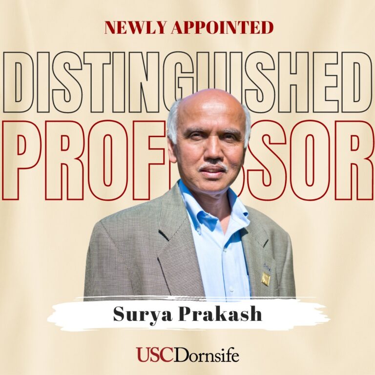
Prof. G. K. Surya Prakash, Organic/Materials
Prof. Richard L. Brutchey, Inorganic
Prof. Vadim Cherezov, Chemical Biology